The starting point is to establish truth tables for the 8 logic symbols:
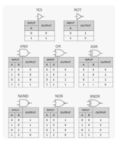
These can now be applied to the circuits.
| A |
B |
C |
NAND-1 |
NAND-2 |
AND-1 |
AND-2 |
NOR-1 |
D |
| 0 |
0 |
0 |
1 |
1 |
1 |
0 |
0 |
1 |
| 0 |
0 |
1 |
1 |
1 |
1 |
0 |
0 |
1 |
| 0 |
1 |
0 |
1 |
1 |
1 |
1 |
0 |
1 |
| 0 |
1 |
1 |
1 |
1 |
1 |
1 |
0 |
1 |
| 1 |
0 |
0 |
1 |
1 |
1 |
0 |
0 |
1 |
| 1 |
0 |
1 |
1 |
0 |
0 |
0 |
1 |
0 |
| 1 |
1 |
0 |
0 |
1 |
0 |
1 |
0 |
1 |
| 1 |
1 |
1 |
0 |
0 |
0 |
0 |
1 |
0 |
This is the main results table with some extra columns for intermediate results (see below).
The circuit diagram shows 3 NAND-gates, 2 AND-gates and 1 NOR-gate. We need to label the gates.
A and B feed NAND-1; A and C feed NAND-2; D is identified as NAND-3; so NAND-1 output=0 only when A=B=1; otherwise it's 1. NAND-1=A NAND B or NAND-1=¬(A∧B).
Similarly A=C=1 make NAND-2 output=0, and any other values make it 1. NAND-2=A NAND C or NAND-2=¬(A∧C).
AND-1 (upmost) =NAND-1 AND NAND-2=1 when NAND-1=NAND-2=1; otherwise 0. AND-1=NAND-1∧NAND-2.
AND-2=B AND NAND-2=1 when B=NAND-2=1; otherwise 0. AND-2=B∧NAND-2.
NOR-1=AND-1 NOR AND-2=1 when AND-1=AND-2=0, otherwise 0. NOR-1=¬(AND-1∨AND-2).
Finally, D=NOR-1 NAND C=0 when NOR-1=C=1; otherwise 1. D=¬(NOR-1∧C).
D=¬(NOR-1∧C)=¬((¬(AND-1∨AND-2))∧C),
D=¬((¬((NAND-1∧NAND-2)∨(B∧NAND-2)))∧C),
D=¬((¬(((¬(A∧B))∧(¬(A∧C)))∨(B∧(¬(A∧C)))))∧C) is the combined Boolean expression.
(See also your other similar question for Boolean notation.)